Team:Grenoble-Alpes/Model
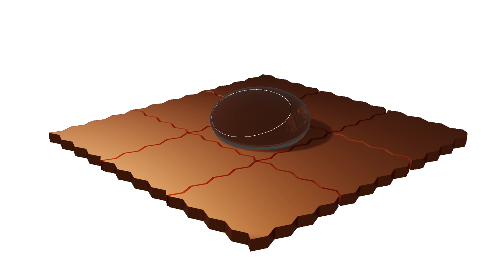
This whole page describes how we modeled some parts of our project. The goal of this page is to give a more profoud understanding of some choices we made or technologies we chose in our project. Some of the parts presented here will be very technical and thus may seem difficult at first sight to understand. It is however quite interesting to have them as some of the technologies we used are quite new and not very documented. This work will thus be a summary of those parts. Electrowetting on Dielectrics or EWOD is a technology used to manipulate small volumes of aqueous solutions, using electronics. The main idea is that, when looking at a sphere, the ratio of the volume per the surface is equal to: This means that by dividing the radius of a sphere per 2, we multiply this ratio per 2. In other words, the forces that only act on the surface of the drop are increased in comparison to the forces that act on the volume. This leads to one simple idea: what if the drop is small enough so that the forces applied on the surface can overcome the forces applied on the volume? And the answer is EWOD. There are many ways to use superficial forces on a drop, but the easiest to use is the electromagnetic force. There are two main ways to see the effect of an electromagnetic field on a drop. The first one is purely mechanical and it is based on one observation: an electromagnetic field leads to a deformation of the surface of the drop. At a certain deformation, the drop will roll. The second one, which we will detail on this page, is based on an energetic vision of the system. The idea of this second vision is to look at where the drop will be more stable, this means where its internal energy will be at the lowest point. And as it happens, this is where the electromagnetic field is highest. Let's first describe the idea. The image above will serve as the basis of the explanation. We have already represented the pads that will serve as tension actuator for EWOD, and we will explain why a little later on this page. In the introduction we said that the reason why this theory worked was because we were working with the different surfaces of the drop. Let’s therefore define the surfaces of our system. Let’s use the subscript L to refer to the drop, S to refer to the surface on which the drop is placed and V the air surrounding the device. We will use the capital letter A to refer to the surfaces. We therefore have three different surfaces on our system: A_LS, A_LV, A_SV. Let’s also represent the volume by the capital letter V and the difference of pressure between the inside of the drop and the outside of the drop. The free energy of the system when no tension is applied is therefore: Now let’s talk about the influence of an electromagnetic field on the drop. The energy stored in an electromagnetic field is defined by: In our system, the electromagnetic energy is stored between the electrode and the drop. If this electromagnetic field is present there it is because the drop and the electrodes are at two different tensions. This is obtained thanks to an insulating film, that we will call dielectric. This film has a thickness that we will represent with the letter d and a relative electrical permittivity represented by the expression Ɛ_d. This formula is a little complex, so let’s simplify it by making some acceptable hypotheses. First, let’s suppose that the drop is an equipotential solid. This means that the drop has the same tension wherever we look. This naturally means that the drop is homogeneous at an ionic level (this hypothesis is an oversimplification due to the little effect that the ions have on the system). With those hypotheses, we can simplify the expression of F_EM: The only parameters that haven’t been presented on this simplified expression of the free energy concealed in the dielectric are U: the difference of tension between the drop and the electrode, and 0, which is the electrical permittivity of the void. This means that the free energy of the system can be written: Because we are working with free energy, the lower it is, the more stable. Naturally, the system will tend to evolve towards its more stable configuration. However, despite the natural tendency of the drop to move, forces will appear that can block the movement. To counterbalance them, we have to make the free energy drop as much as possible when a difference in tension is applied, and we have to reduce as much as possible the friction forces. This means that we have to minimize the surface of the drop that is in contact with the insulating material. This also means that we have to maximize the effect of the difference of tension. Technically, this leads to modifying the surface of the insulating material so it becomes as hydrophobic as possible. This also leads to choosing a dielectric that is as thin as possible. And finally it asks us to use very high tensions. This last point is not totally true as there is a saturation in tension for this phenomenon, which is not yet well described theoretically. In general, this saturation happens a little under 300V. Note that the difference in tension is raised to the square and so we can either use positive or negative tensions, with reference to the drop. In our case, we used positive tensions as it was technically easier to do. The main problem of this technique is that nowadays, it is not common, and therefore the materials we needed to have a perfect system was way too expensive. This forces us to use different techniques to have materials as close to what we need as we can. To conclude this brief presentation of EWOD, we are using changes in tension on pads placed under an insulating material, to move a drop placed on the insulating material. The more hydrophobic the material is, the better, and the thinner the insulator is, the better. The three difficulties of this technique are therefore:
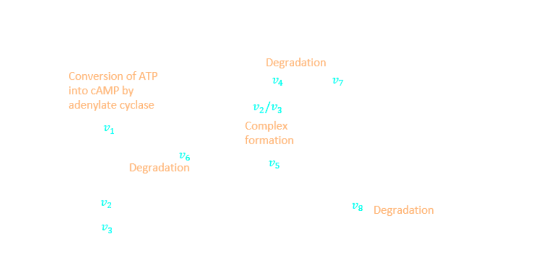
The creation of a mathematical model of the biological system is an important tool for a better understanding and studying of its working. It has the advantage of getting rapid results that can be very accurate, instead of having to do a whole phase of experimentation just to see how the system is responding to the tweaking of a specific parameter. We chose to develop a simple model, where other complex parameters could be added later on to have more elaborate and precise results. The first step is understanding how the system works, and then deciding which part is more important to focus on. In our biological cascade system, we decided to simulate the relationship between the presence of the alpha-synuclein protein in the medium and the output bioluminescent signal. A first model can be described in this way: the presence of alpha-synuclein in the medium triggers the activation of adenylate cyclase, which in turn catalyzes the transformation of ATP to cAMP. The complex CAPcAMP launches the transcription of the nanoluc gene, and therefore, the production of the nanoluciferase. Finally, this enzyme catalyzes the reaction of Furimazine that leads to light production. Many hypotheses, which are backed-up with our experimentation, are considered to simplify the model:
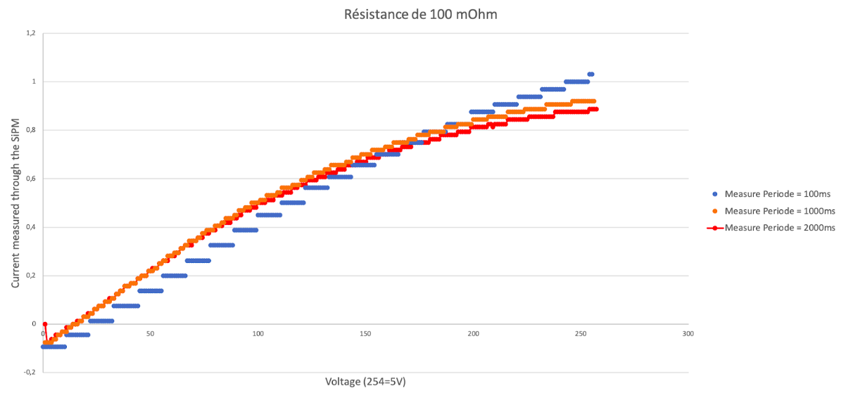
Following these assumptions and using the notations below, we could write the kinetic and mass conservation laws associated to the reactions happening in the system: And finally, we can write the ODE system to be solved: Now, to link the concentration of nanoluciferase to the production of light L, an equation found in the bibliography [2] seems to give the awaited results: Finally, this model is still a first model of this biological cascade, but it can give quite good results. The possibility to add more complex considerations in the model is very large. [1] Sara Berthoumieux et al. “Shared control of gene expression in bacteria by transcription factors and global physiology of the cell”. In:Molecular Systems Biology 9.1 (Jan. 2013), p.634. issn: 1744-4292. doi:10.1038/msb.2012.70. [2] Jolene M. Ignowski and David V. Schaffer. “Kinetic analysis and modeling of firefly luciferase as a quantitative reporter gene in live mammalian cells”. In: Biotechnology and Bioengineering 86.7 (June 2004), pp. 827–834. issn: 00063592. doi: 10.1002/bit.20059. The SiPM is a component that is meant to measure a light intensity or to count electrons. This device is based on a quantum phenomenon called “quantum quench”. This phenomenon describes the exponential increase of a current when a difference of tension is applied. This kind of device is quite rare in modern devices and is used only in some medical devices. Its use is however much more common in astronomy where it is used to detect particles that emit photons when entering our atmosphere (for example neutrinos). A light sensor in electronics is a device that can convert a light intensity into an electrical intensity or an electrical potential. In general we use phototransistors, which are converter that outputs an electrical current. A phototransistor is basically a semiconductor that when is hit by a photon, releases an electron. As a light current is basically a photon flux, the semiconductor releases a flux of electrons when illuminated by a continuous flux of photons. Here we have to clarify the behaviour of the device for different photons. A photon is an elementary particle. To be more precise is an energy quanta associated to electromagnetic waves. This means that it carries the electromagnetic energy. Each photon carries an energy that is linked to its frequency through Einstein-Planck’s equation: E=hc/λ=hν. This entails that the energy of the electron is linked to its “color”. From there we need to describe more in detail the way a phototransistor emits an electron. First, let’s remind that an atom is basically a nucleus and a cloud of electrons orbiting around it. When an electron receives an electromagnetic energy (this means a photon), if the energy is not too low nor too high, it absorbs it and can be pulled apart from the nucleus. This can pull the electron away from the atom, thus sending it through the circuit to which the phototransistor is connected. This means that the behaviour of the phototransistor will depend on the frequency of the light that hits it. In other terms, this will lead to a spectrum of conversion for the device. So as to compare the SiPM to those sensors, let’s take a concrete example of a phototransistor: the SFH 3711 from OSRAM. This sensor allows to theoretically achieve a maximum intensity of 2µA for an incident light intensity of 10µW/cm^2, at 560nm (which is close to what we expect our solution to emit). A SiPM works as a phototransistor up to the point where the electron is emitted. At this point the electron is amplified. The way this is done is through quantum quench. Quantum quench is a phenomenon that happens on specific materials when a difference of potential is applied to a conductor through which a current circulates. The main effect of quantum quench is to amplify the flux of electrons by many orders of magnitudes. As for the phototransistors, a SiPM has a conversion spectrum. In our case we used a C-Series SiPM from OnSemiconductors. This sensor allows theoretically to achieve an intensity of 700mA for an incident light intensity of 10µW/cm^2 at 560nm. This is 350.000 times the current we get from the phototransistor for the same parameters. This is a theoretical value that does not take into account the saturation of the sensor. In fact, with this sensor, we can’t measure more than 15mA. This could be a problem for very bright solutions but for what we are doing it is more than enough. In any case this sensor allows us to be much more precise than with phototransistors. From there, we can look at a more practical approach of the sensor. We just saw that using a SiPM allowed us to be theoretically around 100.000 times more precise than when using a phototransistor. However this is only looking at the analogical signal coming out of the sensor. In our case, we are converting it into a numerical value. The question is therefore: how sensible can we be with this sensor? We decided to use an INA226 to convert the current coming out of the SiPM into a usable numerical value. This means that the limiting component in terms of precision in our device will be this analog to digital converter. To know more about this sensor, check our light sensor page. To see how precise we could be on our measures, we decided to perform a series of tests. As we didn’t find any way to control precisely the light intensity hitting the SiPM, we decided to proceed in two steps. First, we tested the SiPM by connecting it directly to a multimeter. There, we saw that the sensor did saturate at 15mA as predicted, we also saw that it was extremely precise: we placed the detector into an aluminium box, in which we made a hole with a needle. We then fixed the sensor 10 centimeters behind the whole. Then, we used a lamp and observed the evolution of the intensity of the sensor depending on the angle between the hole-sensor axis and the hole-lamp axis. We saw a very noticeable evolution of the measure. We weren’t able to do much more to characterize the sensor but from what we saw, we were pretty confident it would work as predicted. The most important part to characterize was therefore the current sensor. To do so, we used a current generator. This current generator allowed us to calibrate our current sensor so it could give us a result with a precision higher than the minimum we needed. At that point, we had calibrated the current sensor and were sure that our sensor was working. We therefore decided to characterize the device. To characterize a sensor, we usually use a source that delivers the exact amount of what we want to calibrate, and by measuring this output with the sensor we can get an idea of how precise the sensor is. In the case of luminescence, we didn’t find any device capable of getting us to the characterization of the SiPM. We therefore decided to wait for the bioluminescent solution and from there compare the light emitted with a light source that could emit light at lower intensities. What we saw was that the light emitted by the solutions was pretty strong, and a simple LED was delivering a comparable signal. We therefore characterized the sensor with an LED. The idea of this characterization, is to put both the sensor and LED into an opaque chamber, and then apply a progressive difference of potential to the LED, retrieve the current that is returned by the sensor and measure it. To realize the opaque chamber, we used an aluminium cylinder that could be closed. We then used a voltage generator to create the luminous signal on the LED, and we connected the sensor to an arduino that sent the data to the computer. What we got were these curves: From that curve we see that we are able to differentiate nearly every step. However, we have to underline on fact: we need to take the measure on a period of (at minima) 1s to be precise. This is due to the nature of the current sensor. This sensor averages the values by integrating the measure on the measure period. This is why, when using the software, we can’t enter a time between measures lower than 1s. What we see on the curves is that with our device, the lower the light intensity, the most sensible we are. This is a good thing as we are working with bioluminescence and we expect the luminosity to be pretty low. To conclude this characterization, what we can say is that what we used to measure bioluminescence is adapted. ![]() NeuroDrop
NeuroDrop
Model
EWOD (Electrowetting on Dielectric)
Introduction

EWOD Theory


Conclusion
Modeling the Biological System
Modeling the Biological System

Symbol
Definition
xmf
free cAMP concentration
xcf
free CAP concentration
xcm
complex CAPcAMP concentration
xm
total cAMP concentration
xc
total CAP concentration
xl
nanoluciferase concentration
α
alpha-synuclein concentration
a
ATP concentration
kc
maximal synthesis rate of CAP
k+
association rate constant of the complex
k-
dissociation rate constant of the complex
Vm
maximal velocity of Cya
Km
Michaelis constant of Cya
ke
cAMP degradation rate constant
kn
nanoluciferase degradation rate
c
degradation rate constant of CAP and CAPcAMP
n
Hill constant for allosteric regulation of cAMP by alpha-synuclein
m
Hill constant for allosteric regulation of nanoluciferase by CAPcAMP
k
activation constant of cAMP by alpha-synuclein
kcm
binding constant of CAPcAMP to nanoluc promoter
kcat
light production constant (catalytic rate)
RLU
light conversion factor
References
Characterization of the SiPM
Introduction
Theoretical approach to the SiPM
A - Phototransistors
B - SiPM
Experimental approach to the SiPM
Characterization of the SiPM
Conclusion